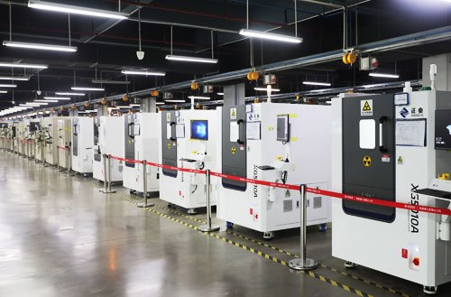
In the process of modern semiconductor chip manufacturing, with the continuous miniaturization of chip structure, traditional detection methods have gradually shown limitations in terms of accuracy, speed and comprehensiveness. Therefore, XRAY (X-ray) detection technology has gradually become an indispensable part of chip manufacturing and quality control. It can use non-destructive detection methods to go deep into the chip and find potential defects, thereby improving the production efficiency and reliability of the chip.
XRAY detection technology generates images of the internal structure of the chip by applying X-rays to the chip with its penetrating properties. Compared with traditional two-dimensional microscope detection, XRAY can obtain three-dimensional internal images to help engineers accurately locate tiny defects and welding problems. For example, XRAY can reveal problems such as voids, cracks or poor contact inside the chip package, discover hidden dangers that may affect chip performance in advance, and prevent bad products from entering the market.
In addition, XRAY detection is widely used in all aspects of chip manufacturing. In chip